TRANSISTOR
A transistor is a semiconductor device used to amplify and switch electronic signals and electrical power. It is composed of semiconductor material with at least three terminals for connection to an external circuit. A voltage or current applied to one pair of the transistor's terminals changes the current flowing through another pair of terminals. Because the controlled (output) power can be higher than the controlling (input) power, a transistor can amplify a signal. Today, some transistors are packaged individually, but many more are found embedded in integrated circuits.
The transistor is the fundamental building block of modern electronic devices, and is ubiquitous in modern electronic systems. Following its development in the early 1950s the transistor revolutionized the field of electronics, and paved the way for smaller and cheaper radios, calculators, and computers, among other things.
Simplified operation
The essential usefulness of a transistor comes from its ability to use a small signal applied between one pair of its terminals to control a much larger signal at another pair of terminals. This property is called gain. A transistor can control its output in proportion to the input signal; that is, it can act as an amplifier. Alternatively, the transistor can be used to turn current on or off in a circuit as an electrically controlled switch, where the amount of current is determined by other circuit elements.
There are two types of transistors, which have slight differences in how they are used in a circuit. A bipolar transistor has terminals labeled base, collector, and emitter. A small current at the base terminal (that is, flowing between the base and the emitter) can control or switch a much larger current between the collector and emitter terminals. For a field-effect transistor, the terminals are labeled gate, source, and drain, and a voltage at the gate can control a current between source and drain.
The image to the right represents a typical bipolar transistor in a circuit. Charge will flow between emitter and collector terminals depending on the current in the base. Since internally the base and emitter connections behave like a semiconductor diode, a voltage drop develops between base and emitter while the base current exists. The amount of this voltage depends on the material the transistor is made from, and is referred to as VBE.
Transistor as a switch
Transistors are commonly used as electronic switches, both for high-power applications such as switched-mode power supplies and for low-power applications such as logic gates.
In a grounded-emitter transistor circuit, such as the light-switch circuit shown, as the base voltage rises, the base and collector current rise exponentially. The collector voltage drops because of the collector load resistance (in this example, the resistance of the light bulb). If the collector voltage were zero, the collector current would be limited only by the light bulb resistance and the supply voltage. The transistor is then said to be saturated - it will have a very small voltage from collector to emitter. Providing sufficient base drive current is a key problem in the use of bipolar transistors as switches. The transistor provides current gain, allowing a relatively large current in the collector to be switched by a much smaller current into the base terminal. The ratio of these currents varies depending on the type of transistor, and even for a particular type, varies depending on the collector current. In the example light-switch circuit shown, the resistor is chosen to provide enough base current to ensure the transistor will be saturated.
In any switching circuit, values of input voltage would be chosen such that the output is either completely off,[21] or completely on. The transistor is acting as a switch, and this type of operation is common in digital circuits where only "on" and "off" values are relevant.
Transistor as an amplifier

The common-emitter amplifier is designed so that a small change in voltage (Vin) changes the small current through the base of the transistor; the transistor's current amplification combined with the properties of the circuit mean that small swings in Vin produce large changes in Vout.
Various configurations of single transistor amplifier are possible, with some providing current gain, some voltage gain, and some both.
From mobile phones to televisions, vast numbers of products include amplifiers for sound reproduction, radio transmission, and signal processing. The first discrete transistor audio amplifiers barely supplied a few hundred milliwatts, but power and audio fidelity gradually increased as better transistors became available and amplifier architecture evolved.
Modern transistor audio amplifiers of up to a few hundred watts are common and relatively inexpensive.
Comparison with vacuum tubes
Prior to the development of transistors, vacuum (electron) tubes (or in the UK "thermionic valves" or just "valves") were the main active components in electronic equipment.
Advantages
The key advantages that have allowed transistors to replace their vacuum tube predecessors in most applications are
- Small size and minimal weight, allowing the development of miniaturized electronic devices.
- Highly automated manufacturing processes, resulting in low per-unit cost.
- Lower possible operating voltages, making transistors suitable for small, battery-powered applications.
- No warm-up period for cathode heaters required after power application.
- Lower power dissipation and generally greater energy efficiency.
- Higher reliability and greater physical ruggedness.
- Extremely long life. Some transistorized devices have been in service for more than 50 years.
- Complementary devices available, facilitating the design of complementary-symmetry circuits, something not possible with vacuum tubes.
- Insensitivity to mechanical shock and vibration, thus avoiding the problem of microphonics in audio applications.
Limitations
- Silicon transistors typically do not operate at voltages higher than about 1000 volts (SiC devices can be operated as high as 3000 volts). In contrast, vacuum tubes have been developed that can be operated at tens of thousands of volts.
- High-power, high-frequency operation, such as that used in over-the-air television broadcasting, is better achieved in vacuum tubes due to improved electron mobility in a vacuum.
- Silicon transistors are much more vulnerable than vacuum tubes to an electromagnetic pulse generated by a high-altitude nuclear explosion.
- Sensitivity to radiation and cosmic rays (special radiation hardened chips are used for spacecraft devices).
- Vacuum tubes create a distortion, the so-called tube sound, that some people find to be more tolerable to the ear.[22]
Types
 |
PNP |
 |
P-channel |
 |
NPN |
 |
N-channel |
| BJT | JFET |
|
|
 |
 |
 |
P-channel |
|
|
 |
 |
 |
N-channel |
| JFET | MOSFET enh | MOSFET dep | ||
Transistors are categorized by
- Semiconductor material (date first used): the metalloids germanium (1947) and silicon (1954)— in amorphous, polycrystalline and monocrystalline form; the compounds gallium arsenide (1966) and silicon carbide (1997), the alloy silicon-germanium (1989), the allotrope of carbon graphene (research ongoing since 2004), etc.—see Semiconductor material
- Structure: BJT, JFET, IGFET (MOSFET), IGBT, "other types"
- Electrical polarity (positive and negative) : NPN, PNP (BJTs); N-channel, P-channel (FETs)
- Maximum power rating: low, medium, high
-
Maximum operating frequency: low, medium, high, radio frequency (RF), microwave (The maximum effective frequency of a transistor is denoted by the term
 , an abbreviation for transition frequency—the frequency of transition is the frequency at which the transistor yields unity gain)
 - Application: switch, general purpose, audio, high voltage, super-beta, matched pair
- Physical packaging: through-hole metal, through-hole plastic, surface mount, ball grid array, power modules—see Packaging
- Amplification factor hfe or βF (transistor beta)[23]
Thus, a particular transistor may be described as silicon, surface mount, BJT, NPN, low power, high frequency switch.
Bipolar junction transistor
Bipolar transistors are so named because they conduct by using both majority and minority carriers. The bipolar junction transistor (BJT), the first type of transistor to be mass-produced, is a combination of two junction diodes, and is formed of either a thin layer of p-type semiconductor sandwiched between two n-type semiconductors (an n-p-n transistor), or a thin layer of n-type semiconductor sandwiched between two p-type semiconductors (a p-n-p transistor). This construction produces two p-n junctions: a base–emitter junction and a base–collector junction, separated by a thin region of semiconductor known as the base region (two junction diodes wired together without sharing an intervening semiconducting region will not make a transistor).
The BJT has three terminals, corresponding to the three layers of semiconductor – an emitter, a base, and a collector. It is useful in amplifiers because the currents at the emitter and collector are controllable by a relatively small base current."[24] In an NPN transistor operating in the active region, the emitter-base junction is forward biased (electrons and electron holes recombine at the junction), and electrons are injected into the base region. Because the base is narrow, most of these electrons will diffuse into the reverse-biased (electrons and holes are formed at, and move away from the junction) base-collector junction and be swept into the collector; perhaps one-hundredth of the electrons will recombine in the base, which is the dominant mechanism in the base current. By controlling the number of electrons that can leave the base, the number of electrons entering the collector can be controlled.[24] Collector current is approximately β (common-emitter current gain) times the base current. It is typically greater than 100 for small-signal transistors but can be smaller in transistors designed for high-power applications.
Unlike the FET, the BJT is a low–input-impedance device. Also, as the base–emitter voltage (Vbe) is increased the base–emitter current and hence the collector–emitter current (Ice) increase exponentially according to the Shockley diode model and the Ebers-Moll model. Because of this exponential relationship, the BJT has a higher transconductance than the FET.
Bipolar transistors can be made to conduct by exposure to light, since absorption of photons in the base region generates a photocurrent that acts as a base current; the collector current is approximately β times the photocurrent. Devices designed for this purpose have a transparent window in the package and are called phototransistors.
Field-effect transistor
The field-effect transistor (FET), sometimes called a unipolar transistor, uses either electrons (in N-channel FET) or holes (in P-channel FET) for conduction. The four terminals of the FET are named source, gate, drain, and body (substrate). On most FETs, the body is connected to the source inside the package, and this will be assumed for the following description.
In a FET, the drain-to-source current flows via a conducting channel that connects the source region to the drain region. The conductivity is varied by the electric field that is produced when a voltage is applied between the gate and source terminals; hence the current flowing between the drain and source is controlled by the voltage applied between the gate and source. As the gate–source voltage (Vgs) is increased, the drain–source current (Ids) increases exponentially for Vgs below threshold, and then at a roughly quadratic rate (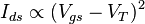 ) (where VT is the threshold voltage at which drain current begins)[25] in the "space-charge-limited" region above threshold. A quadratic behavior is not observed in modern devices, for example, at the 65 nm technology node.[26]
For low noise at narrow bandwidth the higher input resistance of the FET is advantageous.
FETs are divided into two families: junction FET (JFET) and insulated gate FET (IGFET). The IGFET is more commonly known as a metal–oxide–semiconductor FET (MOSFET), reflecting its original construction from layers of metal (the gate), oxide (the insulation), and semiconductor. Unlike IGFETs, the JFET gate forms a p-n diode with the channel which lies between the source and drain. Functionally, this makes the N-channel JFET the solid-state equivalent of the vacuum tube triode which, similarly, forms a diode between its grid and cathode. Also, both devices operate in the depletion mode, they both have a high input impedance, and they both conduct current under the control of an input voltage.
Metal–semiconductor FETs (MESFETs) are JFETs in which the reverse biased p-n junction is replaced by a metal–semiconductor junction. These, and the HEMTs (high electron mobility transistors, or HFETs), in which a two-dimensional electron gas with very high carrier mobility is used for charge transport, are especially suitable for use at very high frequencies (microwave frequencies; several GHz).
Unlike bipolar transistors, FETs do not inherently amplify a photocurrent. Nevertheless, there are ways to use them, especially JFETs, as light-sensitive devices, by exploiting the photocurrents in channel–gate or channel–body junctions.
FETs are further divided into depletion-mode and enhancement-mode types, depending on whether the channel is turned on or off with zero gate-to-source voltage. For enhancement mode, the channel is off at zero bias, and a gate potential can "enhance" the conduction. For depletion mode, the channel is on at zero bias, and a gate potential (of the opposite polarity) can "deplete" the channel, reducing conduction. For either mode, a more positive gate voltage corresponds to a higher current for N-channel devices and a lower current for P-channel devices. Nearly all JFETs are depletion-mode as the diode junctions would forward bias and conduct if they were enhancement mode devices; most IGFETs are enhancement-mode types.
Usage of bipolar and field effect transistors
The bipolar junction transistor (BJT) was the most commonly used transistor in the 1960s and 70s. Even after MOSFETs became widely available, the BJT remained the transistor of choice for many analog circuits such as amplifiers because of their greater linearity and ease of manufacture. In integrated circuits, the desirable properties of MOSFETs allowed them to capture nearly all market share for digital circuits. Discrete MOSFETs can be applied in transistor applications, including analog circuits, voltage regulators, amplifiers, power transmitters and motor drivers.
Other transistor types
| This article contains embedded lists that may be poorly defined, unverified or indiscriminate. (September 2009) |
-
Bipolar junction transistor
- Heterojunction bipolar transistor, up to several hundred GHz, common in modern ultrafast and RF circuits
- Schottky transistor
- Avalanche transistor
- Darlington transistors are two BJTs connected together to provide a high current gain equal to the product of the current gains of the two transistors.
- Insulated gate bipolar transistors (IGBTs) use a medium power IGFET, similarly connected to a power BJT, to give a high input impedance. Power diodes are often connected between certain terminals depending on specific use. IGBTs are particularly suitable for heavy-duty industrial applications. The Asea Brown Boveri (ABB) 5SNA2400E170100 illustrates just how far power semiconductor technology has advanced.[27] Intended for three-phase power supplies, this device houses three NPN IGBTs in a case measuring 38 by 140 by 190 mm and weighing 1.5 kg. Each IGBT is rated at 1,700 volts and can handle 2,400 amperes.
- Photo transistor
- Multiple-emitter transistor, used in transistor–transistor logic
- Multiple-base transistor, used to amplify very low level signals in noisy environments such as the pickup of a record player or radio front ends. Effectively, it is a very large number of transistors in parallel where, at the output, the signal is added constructively, but random noise is added only stochastically.[28]
-
Field-effect transistor
- Carbon nanotube field-effect transistor (CNFET)
- JFET, where the gate is insulated by a reverse-biased p-n junction
-
MESFET, similar to JFET with a Schottky junction instead of a p-n junction
- High Electron Mobility Transistor (HEMT, HFET, MODFET)
- MOSFET, where the gate is insulated by a shallow layer of insulator
- Inverted-T field effect transistor (ITFET)
- FinFET, source/drain region shapes fins on the silicon surface.
- FREDFET, fast-reverse epitaxial diode field-effect transistor
- Thin film transistor, in LCDs.
- OFET Organic Field-Effect Transistor, in which the semiconductor is an organic compound
- Ballistic transistor
- Floating-gate transistor, for non-volatile storage.
-
FETs used to sense environment
- Ion-sensitive field effect transistor, to measure ion concentrations in solution.
- EOSFET, electrolyte-oxide-semiconductor field effect transistor (Neurochip)
- DNAFET, deoxyribonucleic acid field-effect transistor
- Diffusion transistor, formed by diffusing dopants into semiconductor substrate; can be both BJT and FET
- Unijunction transistors can be used as simple pulse generators. They comprise a main body of either P-type or N-type semiconductor with ohmic contacts at each end (terminals Base1 and Base2). A junction with the opposite semiconductor type is formed at a point along the length of the body for the third terminal (Emitter).
- Single-electron transistors (SET) consist of a gate island between two tunneling junctions. The tunneling current is controlled by a voltage applied to the gate through a capacitor.[29]
- Nanofluidic transistor, controls the movement of ions through sub-microscopic, water-filled channels.[30]
-
Multigate devices
- Tetrode transistor
- Pentode transistor
- Trigate transistors (Prototype by Intel)
- Dual gate FETs have a single channel with two gates in cascode; a configuration optimized for high frequency amplifiers, mixers, and oscillators.
- Junctionless Nanowire Transistor (JNT), developed at Tyndall National Institute in Ireland, was the first transistor successfully fabricated without junctions. (Even MOSFETs have junctions, although its gate is electrically insulated from the region the gate controls.) Junctions are difficult and expensive to fabricate, and, because they are a significant source of current leakage, they waste significant power and generate significant waste heat. Eliminating them held the promise of cheaper and denser microchips. The JNT uses a simple nanowire of silicon surrounded by an electrically isolated "wedding ring" that acts to gate the flow of electrons through the wire. This method has been described as akin to squeezing a garden hose to gate the flow of water through the hose. The nanowire is heavily n-doped, making it an excellent conductor. Crucially the gate, comprising silicon, is heavily p-doped; and its presence depletes the underlying silicon nanowire thereby preventing carrier flow past the gate.
- Vacuum channel transistor: In 2012, NASA and the National Nanofab Center in South Korea were reported to have built a prototype vacuum channel transistor in only 150 nanometers in size, can be manufactured cheaply using standard silicon semiconductor processing, can operate at high speeds even in hostile environments, and could consume just as much power as a standard transistor.[31]
Part numbers
| Beginning of Part Number | Type of Transistor |
|---|---|
| 2SA | high frequency PNP BJTs |
| 2SB | audio frequency PNP BJTs |
| 2SC | high frequency NPN BJTs |
| 2SD | audio frequency NPN BJTs |
| 2SJ | P-channel FETs (both JFETs and MOSFETs) |
| 2SK | N-channel FETs (both JFETs and MOSFETs) |
The types of some transistors can be parsed from the part number. There are three major semiconductor naming standards; in each the alphanumeric prefix provides clues to type of the device.
The Japanese Industrial Standard (JIS) JIS-C-7012 standard for transistor part numbers starts with "2S",[32] e.g. 2SD965, but sometimes the "2S" prefix is not marked on the package – a 2SD965 might only be marked "D965"; a 2SC1815 might be listed by a supplier as simply "C1815". This series sometimes has suffixes (such as "R", "O", "BL"... standing for "Red", "Orange", "Blue" etc.) to denote variants, such as tighter hFE (gain) groupings.
The Pro Electron part numbers begin with two letters: the first gives the semiconductor type (A for germanium, B for silicon, and C for materials like GaAs); the second letter denotes the intended use (A for diode, C for general-purpose transistor, etc.). A 3-digit sequence number (or one letter then 2 digits, for industrial types) follows. With early devices this indicated the case type. Suffixes may be used, with a letter (e.g. "C" often means high hFE, such as in: BC549C[33]) or other codes may follow to show gain (e.g. BC327-25) or voltage rating (e.g. BUK854-800A[34]). The more common prefixes are:
| Prefix class | Usage | Example |
|---|---|---|
| AC | Germanium small signal transistor | AC126 |
| AF | Germanium RF transistor | AF117 |
| BC | Silicon, small signal transistor ("allround") | BC548B |
| BD | Silicon, power transistor | BD139 |
| BF | Silicon, RF (high frequency) BJT or FET | BF245 |
| BS | Silicon, switching transistor (BJT or MOSFET) | BS170 |
| BL | Silicon, high frequency, high power (for transmitters) | BLW34 |
| BU | Silicon, high voltage (for CRT horizontal deflection circuits) | BU508 |
The JEDEC EIA370 transistor device numbers usually start with "2N", indicating a three-terminal device (dual-gate field-effect transistors are four-terminal devices, so begin with 3N), then a 2, 3 or 4-digit sequential number with no significance as to device properties (although early devices with low numbers tend to be germanium). For example 2N3055 is a silicon NPN power transistor, 2N1301 is a PNP germanium switching transistor. A letter suffix (such as "A") is sometimes used to indicate a newer variant, but rarely gain groupings.
Other schemes
Manufacturers of devices may have their own proprietary numbering system, for example CK722. Note that a manufacturer's prefix (like "MPF" in MPF102, which originally would denote a Motorola FET) now is an unreliable indicator of who made the device. Some proprietary naming schemes adopt parts of other naming schemes, for example a PN2222A is a (possibly Fairchild Semiconductor) 2N2222A in a plastic case (but a PN108 is a plastic version of a BC108, not a 2N108, while the PN100 is unrelated to other xx100 devices).
Military part numbers sometimes are assigned their own codes, such as the British Military CV Naming System.
Manufacturers buying large numbers of similar parts may have them supplied with "house numbers", identifying a particular purchasing specification and not necessarily a device with a standardized registered number. For example, an HP part 1854,0053 is a (JEDEC) 2N2218 transistor[35][36] which is also assigned the CV number: CV7763[37]
Naming problems
With so many independent naming schemes, and the abbreviation of part numbers when printed on the devices, ambiguity sometimes occurs. For example two different devices may be marked "J176" (one the J176 low-power Junction FET, the other the higher-powered MOSFET 2SJ176).
As older "through-hole" transistors are given Surface-Mount packaged counterparts, they tend to be assigned many different part numbers because manufacturers have their own systems to cope with the variety in pinout arrangements and options for dual or matched NPN+PNP devices in one pack. So even when the original device (such as a 2N3904) may have been assigned by a standards authority, and well known by engineers over the years, the new versions are far from standardized in their naming.
Construction
Semiconductor material
|
Semiconductor material |
Junction forward voltage V @ 25 °C |
Electron mobility m2/(V·s) @ 25 °C |
Hole mobility m2/(V·s) @ 25 °C |
Max. junction temp. °C |
|---|---|---|---|---|
| Ge | 0.27 | 0.39 | 0.19 | 70 to 100 |
| Si | 0.71 | 0.14 | 0.05 | 150 to 200 |
| GaAs | 1.03 | 0.85 | 0.05 | 150 to 200 |
| Al-Si junction | 0.3 | — | — | 150 to 200 |
The first BJTs were made from germanium (Ge). Silicon (Si) types currently predominate but certain advanced microwave and high performance versions now employ the compound semiconductor material gallium arsenide (GaAs) and the semiconductor alloy silicon germanium (SiGe). Single element semiconductor material (Ge and Si) is described as elemental.
Rough parameters for the most common semiconductor materials used to make transistors are given in the table to the right; these parameters will vary with increase in temperature, electric field, impurity level, strain, and sundry other factors.
The junction forward voltage is the voltage applied to the emitter-base junction of a BJT in order to make the base conduct a specified current. The current increases exponentially as the junction forward voltage is increased. The values given in the table are typical for a current of 1 mA (the same values apply to semiconductor diodes). The lower the junction forward voltage the better, as this means that less power is required to "drive" the transistor. The junction forward voltage for a given current decreases with increase in temperature. For a typical silicon junction the change is −2.1 mV/°C.[38] In some circuits special compensating elements (sensistors) must be used to compensate for such changes.
The density of mobile carriers in the channel of a MOSFET is a function of the electric field forming the channel and of various other phenomena such as the impurity level in the channel. Some impurities, called dopants, are introduced deliberately in making a MOSFET, to control the MOSFET electrical behavior.
The electron mobility and hole mobility columns show the average speed that electrons and holes diffuse through the semiconductor material with an electric field of 1 volt per meter applied across the material. In general, the higher the electron mobility the faster the transistor can operate. The table indicates that Ge is a better material than Si in this respect. However, Ge has four major shortcomings compared to silicon and gallium arsenide:
- Its maximum temperature is limited;
- it has relatively high leakage current;
- it cannot withstand high voltages;
- it is less suitable for fabricating integrated circuits.
Because the electron mobility is higher than the hole mobility for all semiconductor materials, a given bipolar NPN transistor tends to be swifter than an equivalent PNP transistor type. GaAs has the highest electron mobility of the three semiconductors. It is for this reason that GaAs is used in high frequency applications. A relatively recent FET development, the high electron mobility transistor (HEMT), has a heterostructure (junction between different semiconductor materials) of aluminium gallium arsenide (AlGaAs)-gallium arsenide (GaAs) which has twice the electron mobility of a GaAs-metal barrier junction. Because of their high speed and low noise, HEMTs are used in satellite receivers working at frequencies around 12 GHz.
Max. junction temperature values represent a cross section taken from various manufacturers' data sheets. This temperature should not be exceeded or the transistor may be damaged.
Al–Si junction refers to the high-speed (aluminum–silicon) metal–semiconductor barrier diode, commonly known as a Schottky diode. This is included in the table because some silicon power IGFETs have a parasitic reverse Schottky diode formed between the source and drain as part of the fabrication process. This diode can be a nuisance, but sometimes it is used in the circuit.
Packaging
Discrete transistors are individually packaged transistors. Transistors come in many different semiconductor packages (see image). The two main categories are through-hole (or leaded), and surface-mount, also known as surface mount device (SMD). The ball grid array (BGA) is the latest surface mount package (currently only for large integrated circuits). It has solder "balls" on the underside in place of leads. Because they are smaller and have shorter interconnections, SMDs have better high frequency characteristics but lower power rating.
Transistor packages are made of glass, metal, ceramic, or plastic. The package often dictates the power rating and frequency characteristics. Power transistors have larger packages that can be clamped to heat sinks for enhanced cooling. Additionally, most power transistors have the collector or drain physically connected to the metal enclosure. At the other extreme, some surface-mount microwave transistors are as small as grains of sand.